Utilization of Dynamic Nanoindentation for Soft Materials
Junghyun Cho, Hyungsuk Lee*, Babak Arfaei*, and
Dongmyung Suh*
State University of New York (SUNY), Binghamton, New York 13902-6000
*Graduate student
Overview:
The proposed study aims to develop nanoindentation techniques in order to accurately probe mechanical behavior of soft materials used in packaging. This work focuses on polymers (parylene C, PDMS) and solder materials (Sn-Ag-Cu, Pb-Sn). One goal is to extend our understanding of the nanoindentation mechanics and its measurement techniques to soft materials that draw special attention due to their significant time- and temperature-dependent deformation.
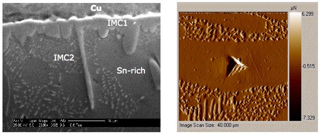
Polymers occupy a significant fraction of packaging materials and their share is expected to grow further. In addition, Pb-free solder will soon dominate a metallic interconnect market by replacing traditional Pb-Sn solders. There are, however, many unknown factors in mechanical behavior of Pb-free solders. From our previous studies, it was clear that these materials would create significant challenges to obtain accurate determination of mechanical properties through nanoindentation. It is because they are too soft and the contact response is distinct from that of time-independent metals or ceramics.
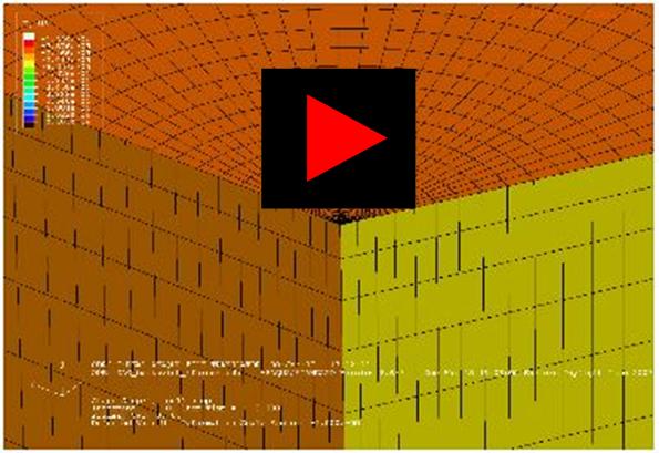
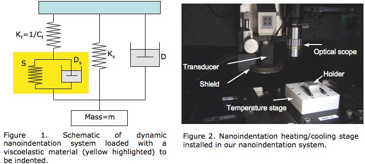
A better mechanistic understanding of the temporal mechanical response would thus be essential to achieve more reliable nanoindentation testing protocol for soft materials (Fig.1). Further, testing of these materials under ambient conditions no longer provides accurate data if they are to be exposed to high temperatures. In-situ mechanical testing under the condition that emulates elevated temperature environments needs to be implemented for evaluation of the materials (Fig.2).
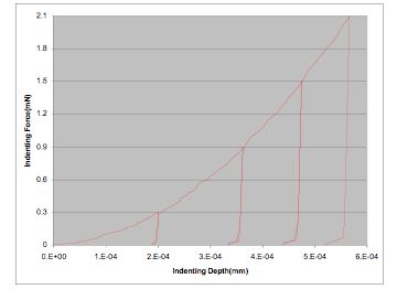
The purpose of this work is to develop accurate dynamic nanoindentation that can resolve the aforementioned issues frequently found in soft materials. Dynamic testing is carried out by superimposing a small, sinusoidally varying (i.e., AC) signal on top of a DC signal that drives the motion of the indenter. Such dynamic testing has been done via a dynamic mechanical analysis (DMA) test on the macroscopic scale; however, the nanoindentation testing can provide it on the nano- and microscales at specific locations. This technique not only offers enough sensitivity to detect materials response from soft surfaces, but also differentiate actual material response from the measurement artifacts such as a thermal drift during indentation.
In order to supplement experimental approaches, the nanoindentation simulation is being developed. For this purpose, the ABAQUS is used to implement finite element analysis of indentation modeling. This work also seeks to develop a constitutive model for the Pb-free solder that incorporates both elastic and plastic deformation including the effects of grain size, applied stress, temperature, and strain rate. The combined analyses from experiments and simulation undertaken here will not only be useful in better understanding certain experimental observations, but also provide a guide for the development of the nanoindentation testing and mechanics.
Sample Results:
Support for this project is provided by Integrated
Electronics Engineering Center (IEEC).